Thin Film Deposition Techniques
The thin film deposition industry has seen some amazing innovations and improvements that have led to the development of fast, scalable, highly efficient deposition setups. In this blog, we will discuss prevalent chemical vapor deposition and physical vapor deposition techniques and applications.
What is thin film deposition?
Thin film deposition techniques are used to modify the surface properties of engineering components by applying thin (< 1 micron) material coatings. These modifications are quite diverse, able to affect material characteristics such as conductivity, wear, fatigue, corrosion, hardness, and much more (depending on your application needs). Common thin film applications include:
- Electronic components and displays
- Solid surface coatings
- Biomedical
- Optical coating
- Data storage devices
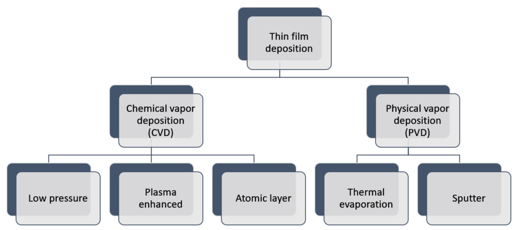
While there are many thin film deposition techniques out there, we will only focus on those in Figure 1.
Physical vapor deposition (PVD)
As the name suggests, physical vapor deposition utilizes a physical process to deposit thin films. The material to be deposited (target material) is first vaporized from a solid form into plasma or ions. The target material is then transferred to the substrate surface and allowed to condense and grow into a film.
Thermal evaporation
Thermal evaporation works by vaporizing the target material using thermal energy from a tungsten heating element or an electron beam. After vaporization, the material is transported through a high pressure vacuum (1 x 10‑6 to 1 x 10‑9 Torr) and is deposited onto the substrate where it condenses and grows into a solid film.
This method can be used to deposit pure metals, non‑metals, oxides, and nitrides. It is most often used to deposit electrically conductive metallic layers on solar cells, OLED displays, and thin‑film transistors.
Sputtering deposition
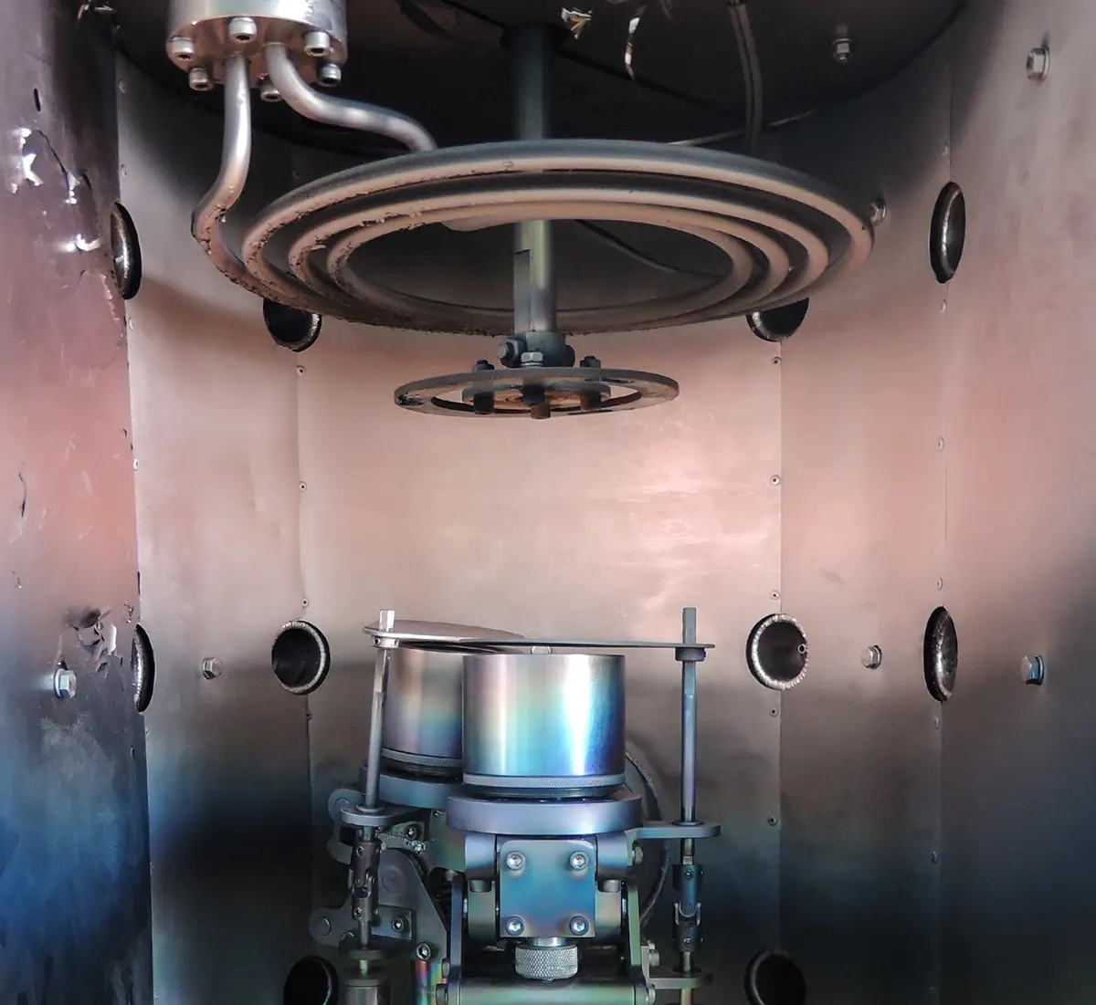
Sputtering deposition works by transferring ions from a target material onto a substrate material using plasma, often argon, in a vacuum chamber (0 – 0.03 Torr).
While sputtering deposition techniques vary in their specifics, the basic setup and operation follows. The target material is connected to a negatively charged cathode, and the substrate is connected to a positively charged anode. Free electrons accelerate toward the anode and collide with the argon atoms, converting them into positively charged ions. The argon ions then accelerate toward the cathode and collide with the target material, releasing atoms which are deposited onto the substrate surface.
Sputtering deposition found its earliest application in production of computer hard disks and is now used extensively in integrated circuit processing, production of anti‑reflective or high emissivity film coated glass, cutting tool coatings, and coating of CDs and DVDs.
Chemical vapor deposition (CVD)
In chemical vapor deposition, a thin film is produced via chemical reaction, usually with a gaseous target material that reacts near the substrate to produce the desired thin film. CVD processes use mass flow controllers to introduce precise amounts of gas reactants to a process chamber. The reactants are then transported to the substrate surfaces, where the chemical reaction takes place and the substrate adsorbs the desired reaction product. Any additional chemical by‑products are desorbed and removed.
Low pressure chemical vapor deposition (LPCVD)
Low pressure chemical vapor deposition is performed at pressures of 0.1 – 10 Torr and temperatures ranging from 200 – 800°C. The reactants are added to the chamber using a specialized precursor delivery system shower head. The shower head and the chamber walls are cooled and the substrate is heated, to promote heterogeneous surface reactions. Once the reaction is complete, the by‑products are removed using the vacuum pumps.
LPCVD is most commonly used in the production of resistors, capacitor dielectrics, MEMS, and anti‑reflective coatings.
Plasma enhanced chemical vapor deposition (PECVD)
Plasma enhanced chemical vapor deposition uses plasma to provide the energy required to facilitate the chemical reaction that drives the deposition. Electrical energy is used to create this neutral gas plasma. PECVD is performed at 2 – 10 Torr and relatively low temperatures from 200 – 400°C.
PECVD is widely used in the production of solar cells and microelectronics. As PECVD is performed at relatively lower temperatures, it allows the use of substrates that are not able to sustain the higher temperatures present in other CVD techniques.
Atomic layer deposition (ALD)
Atomic layer deposition generally uses two precursors that react with the substrate’s surface sequentially. The thin film is deposited by alternating the precursors fed to the chamber. This allows the user to deposit the desired thin film layer by layer and provides much better control over the film thickness.
ALD is commonly used in the fabrication of microelectronics. Several products that use ALD include magnetic recording heads, MOSFET gate stacks, DRAM capacitors, and nonvolatile ferroelectric memories. It is also used to modify surface properties of biomedical devices that are implanted into the body.
Conclusion
When considering the most appropriate thin film deposition method for your application, it is critical to understand the available processes so you can choose the one that will maximize the quality and throughput of your coatings.
With a 10 ms response time, accuracy as good as 0.5% of reading, and the ability to easily fit into your pre‑existing setup, Alicat’s MCE or MCV‑Series mass flow controllers can be used to produce high quality, repeatable coatings in a variety of deposition setups.